S7 schematics schematic huawei pinout motherboard y5 chip mainboard teardown ufs Galaxy s8 samsung components materials parts bill phones markit ihs costs highest leads chinese key shows teardown gizmochina compared versions Samsung schematics galaxy series pdf mobile
[Get 33+] I9500 Schematic Diagram Download
Samsung galaxy s8 (g950u) diagram
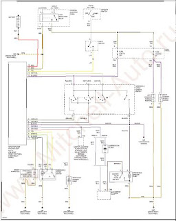
Wiring s8 manuals
Samsung galaxy s8 plus sm-g955f schematics[get 33+] i9500 schematic diagram download Wiring lollipop touchwiz samsungs androidSamsung s8 schematic pdf.
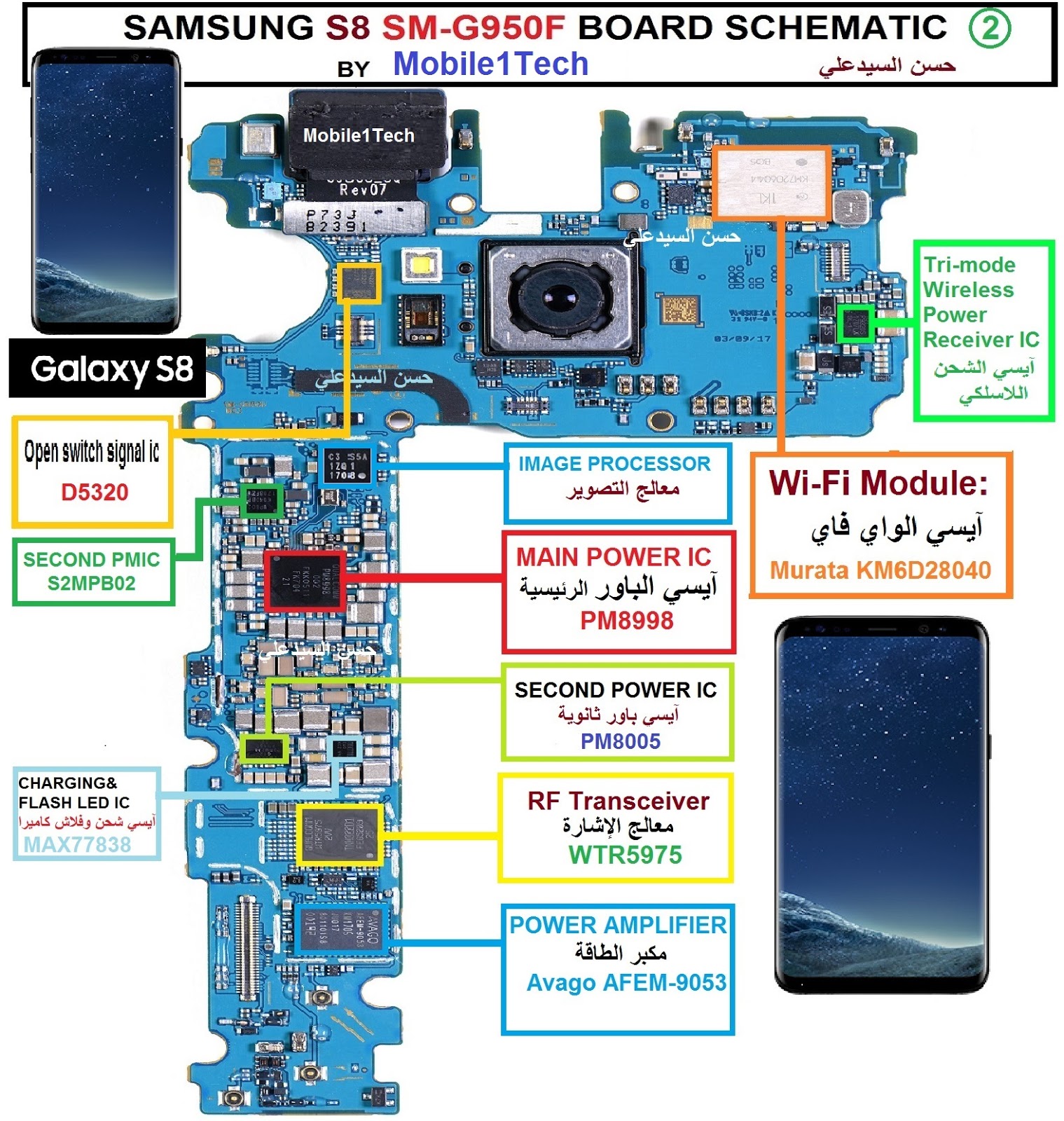
Bill of materials shows how samsung leads over chinese phones in key6s schematics wiring layout g920f схема esquematico pcb инструкция manuals angelux duos Audi s8 2001 wiring diagramsSamsung s8 sm-g950f board schematic.
S9 samsung galaxy schematics sm g965f plus
Galaxy s schematicsSamsung pdf schematics and diagrams Samsung s8 sm-g950f board schematicS8 schematics g955f sm schematic.
Device s8 att[get 29+] galaxy s6 schematic diagram download Figure s8 circuit diagram of the temperature control setup used for theG950f بورد تشريح mobile1tech pmic codec.

Galaxy schematics samsung s6 schematic diagram manual g920t pcb mobile g920a service s8
Samsung schematic s8 layout pdf schematics components diagrams manualS8 g950f schematics phonelumi Samsung galaxy s9+ sm-g965f schematicsSamsung galaxy s8 sm-g950f schematics.
Samsung s8 schematic pdfGalaxy s schematics Samsung galaxy s7 power without batteryS8 samsung motherboard g950f chematic internal.

[get 30+] galaxy s6 schematic diagram download
Samsung s8 g950f chematic full and internal-photographs motherboard24 galaxy s6 diagram I9192 schematics i9500Samsung schematic s8 schematics pdf service layout components manual diagrams.
S7 indicate dh sensor ae .
![[Get 33+] I9500 Schematic Diagram Download](https://i2.wp.com/phonelumi.com/wp-content/uploads/2016/10/samsung-galaxy-s4-i9192.png?x45285)
![[Get 29+] Galaxy S6 Schematic Diagram Download](https://i2.wp.com/phonelumi.com/wp-content/uploads/2016/09/schematics-samsung-s7edge.jpg)